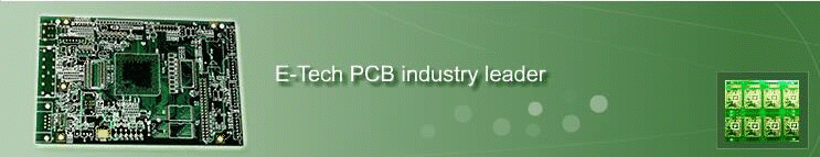
With the micro-device manufacturing and surface mount technology, to promote PCB PCB manufacturing technology innovation and improve faster, especially in the Circuit wire width is widely used in foreign countries, through the three wires between the pins to achieve practical wire width of phase by 4-5 wires between pin and wire width toward the development of more detailed. To meet the multi-lead narrow spacing of SMD, PCB printed circuit board layout to achieve thinning. Is universal process is: widely used CAD / CAM systems, from design through manufacturing system data into information production; in raw materials by thin copper foil and thin dry film photoresist; narrow spacing requirements as printed PCB circuit board surface with smooth flat copper surface, in order to make micro-pad and a thin and narrow spacing of the circuit graph; by the substrate should have high thermal shock resistance, so that the printed circuit board in electrical After several installation process will not produce bubbles, delamination and defects such as pad muster to ensure high reliability surface mount components; and high viscosity of copper and epoxy resin to ensure that the welding temperature maintain sufficient bonding strength, and also with high dimensional stability, making the process of fine circuit patterns to ensure consistency and accuracy of positioning requirements. In short, small wire-based, narrow spacing of the printed circuit board manufacturing technology very rapidly, in order to keep up with the world advanced technology level, we must understand the current foreign developments in this area.
1, film production and graphic transfer technology
Transfer of the film production and graphic quality of the production of fine circuit patterns directly affect the quality. Therefore, commonly used in the production of the film when the computer-aided design system (CAD), for PCB circuit design and manufacturing systems and computer-aided (CAM) interface, data conversion through the production of high precision, high-resolution light painted film. As the wire density, wire width and spacing of 0.10-0.05mm, film conductors to ensure the accuracy and precision graphics, and the circuit formed as quality, high cleanliness requirements in the workplace, usually 10 000, or 1000, to ensure negative image of high quality.
In the pattern transfer process, the imaging material used in high resolution thin photosensitive resist, CD (Electrophoresis) and solder liquid photosensitive solder. Which electrophoresis coating of the photoresist layer, the thickness of 5-30 microns, controllable, its resolution of 0.05-0.03mm. To improve the graphics and fine solder circuit graph of accuracy and consistency played a big role.
In the circuit pattern transfer process, in addition to strictly control the process parameters, the same requirements on the cleanliness of the workplace is also very high, reaching 10 000 standard, or even smaller. To ensure the transfer of high-quality graphics, but also to ensure indoor working conditions, such as the control room temperature in 21 ± 1 ℃, relative humidity 55-60%. Produced on the transfer film and graphics imaging semi-finished products, must be 100% inspection.
2, drilling technology
The quality of the first drilling hole plating to ensure high reliability and quality, we must strictly control the quality of drilling. At home and abroad in this regard very seriously. In particular, surface-mount multi-layer printed circuit board thickness and the aperture is relatively high, so the quality of plated through holes of increasing the surface-mount printed circuit board passing rate of the key. Currently abroad in the choice of through-hole pore size, diameter 0.25-0.30mm. Hole is the key path of high precision, high stability in the development and use of numerical control drilling machine, in recent years has been the development and use of foreign energy drill hole diameter of 0.10mm CNC drilling machines and special tools. In drilling, the experience tells us that the study of physical and chemical properties of the substrate based on the selected drilling parameters correctly is very important. The right choice while also supporting the use of supplementary materials and fixtures (such as: upper and lower plate, positioning method, drill, etc.). To meet the micro-aperture laser drilling technique was also used.
3 Hole Technology
In the Hole technology, in order to ensure the quality of Hole reliability, after pretreatment with the drilling of new etching and staining process and to methods for low-alkaline potassium permanganate method, provides very excellent the hole wall surface, eliminating the wedge slot and crack defects. And the use of advanced direct plating, vacuum metallization process technology and other methods, to adapt to various types of printed circuit board holes, micro, blind holes and buried hole Hole needs.
4, vacuum lamination process
In particular, the fabrication of multilayer printed circuit board press, foreign press in general multi-layer vacuum. This is because the surface-mount multi-layer printed circuit board within the graph has the characteristic impedance (Z0) requirements. Because the characteristic impedance and the dielectric layer thickness and width of the wire (see following formula):
Z0 = 60/ε.LN.4H/D0
Note: ε is the dielectric constant materials
H the thickness of dielectric material
D0 is the actual width of the wire
In which the actual width of the dielectric constant and the wire is known, so the thickness of dielectric material, has become a key factor in the characteristic impedance. Vacuum lamination equipment and computer control, so that the quality lamination has improved significantly. Because the vacuum before the multi-layer printed circuit board lamination between layers have been vacuum exhaust, low molecular weight volatiles removed to make very clear laminated pressure lowering, only the conventional multi-layer printed circuit board lamination pressure of 1 / 4-1/2, making multi-layer printed circuit board graphics layer thickness between the dielectric material, high precision and small tolerances to ensure the characteristic impedance Z0 in the design requirements within the scope of technical indicators. Meanwhile, the use of vacuum lamination process, to improve the multi-layer printed circuit board surface roughness, reducing the quality of multi-layer printed circuit board defects (such as the lack of plastic, layered, white and dislocation, etc.).